A*STAR's advanced packaging lab has drawn 50 companies and S$46m. Applied Materials is expanding it
Phase 4 of the advanced packaging joint lab follows five years in which nine local SMEs ran R&D projects through the program, alongside new A*STAR tie-ups with KLA, STATS ChipPAC and GlobalFoundries.
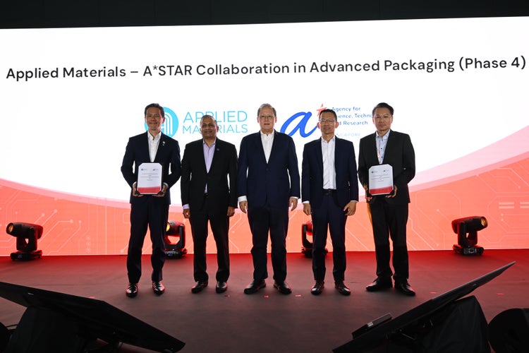
Fifty companies, nine of them local SMEs, have run R&D projects worth S$46 million in industry funding through Applied Materials' advanced packaging joint laboratory with Singapore's Agency for Science, Technology and Research (A*STAR) over the past five years, according to Minister for Trade and Industry (Energy and Industry) Dr Tan See Leng.
Tan announced the phase four of the partnership at the Innovate Together forum on September 25, calling it one of Applied Materials' largest R&D investments in Singapore to date. He said the expansion would significantly increase the lab's infrastructure, equipment and headcount.
"Advanced packaging is one area where public-private partnerships have produced encouraging results, including spillovers to the wider ecosystem," Tan said.
The lab has run since 2011 through three phases. Applied Materials has launched more than 10 semiconductor manufacturing tools developed in Singapore through it, most of which have become global bestsellers, according to Tan, with the ministry naming Ventura, InVia 2 and Kinex among them.
Three more routes into A*STAR's advanced packaging work
A*STAR will set up a joint lab with KLA, the US company whose inspection and measurement tools chipmakers use to find defects during production. The lab will develop process control solutions that catch those defects earlier, according to the ministry, and will sit with A*STAR’s Institute of Microelectronics. KLA is partway through a US$200 million expansion of its own Singapore operations, due to reach 420,000 square feet this year.
STATS ChipPAC will combine A*STAR technologies with its own manufacturing capabilities in co-packaged optics, which the ministry said would build a pathway towards high-volume production. Co-packaged optics moves the optical components into the chip package itself, enabling faster and more energy-efficient data movement inside AI data centres.
In silicon photonics, GlobalFoundries and A*STAR will work on next-generation technologies built on 300-millimetre wafers for high-performance computing and, potentially, quantum applications. For context, the two have worked together since 2017, when A*STAR spun off Advanced Micro Foundry. Tan said the company's manufacturing assets, intellectual property and talent were what attracted GlobalFoundries to acquire it in 2025.
Tacta Systems will develop MEMS sensing technologies for robotics through A*STAR's Lab-in-Fab platform, which the ministry describes as letting companies develop and validate technologies in a production-relevant environment before scaling them. Tacta has also opened its Singapore operations.
Talent routes widen
Tan named talent as the second of two priorities for the sector, alongside industry partnerships.
The Singapore Institute of Technology will pilot a "2+2" model from September 2027, under which students spend two years on campus and almost two years in workplace immersion. At postgraduate level, 14 semiconductor companies have taken part in the Industrial Postgraduate Program over the past five years, producing close to 100 graduates.
The announcements were made under SG Semiconductor, a national identity for the sector developed jointly by A*STAR and the Singapore Economic Development Board (EDB). A*STAR said the brand is intended to raise global visibility of Singapore's capabilities and make the ecosystem easier for companies and talent to navigate, and that the effort will focus on public sector R&D first.
"As semiconductor technologies become more complex, companies are increasingly seeking trusted locations where innovation, manufacturing and talent come together," said Jermaine Loy, managing director of EDB.
Singapore accounts for about one in ten chips produced globally and one in five pieces of semiconductor manufacturing equipment, according to the ministry. Its seven priority technology areas span advanced packaging, silicon photonics, power electronics, radio frequency gallium nitride, piezoMEMS, flat optics and integrated circuit design, supported by the S$800 million RIE Flagship in Semiconductors announced earlier this year, which runs to 2030.